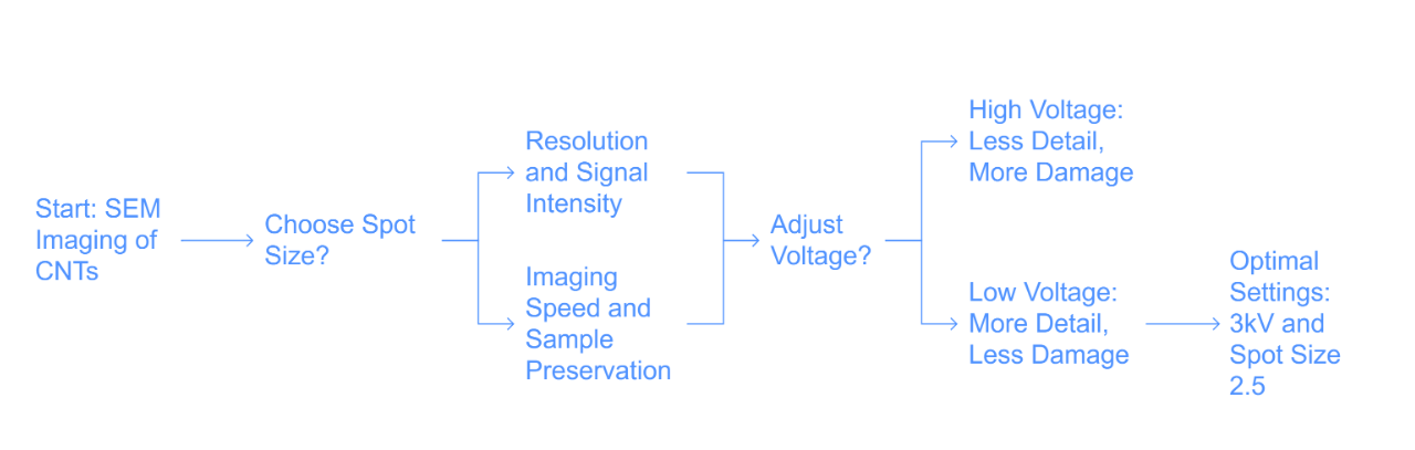
Scanning electron microscopy (SEM) is a method used to characterize 2D and 3D materials morphologically. It is of great importance with its high resolution, especially in the characterization of nano- and micro-sized materials. In this study, carbon nanotubes (CNTs) were analyzed with SEM, and high-quality images were obtained. With SEM analysis, it can be seen whether carbon nanotubes are formed in a regular structure or not, and whether there are agglomerations or distortions in the structure and could also be utilized to quantify the degree of purity within samples. The diameters of carbon nanotubes can be measured using SEM images. This study obtained the best imaging parameters by taking many SEM images at different magnifications under 3.5 and 7 kV voltage and 2, 2.5, and 3 spot values. The results showed that in the characterization of CNTs by SEM, low spot and low voltage values are more suitable for detailed surface morphology imaging and obtaining high resolution.
Yardimci AI, Acikbas Y, Capan R. SEM images of carbon nanotubes (CNTs): Effect of voltage and spot size on image resolutions, Res. Des. 2024; 1(1): 43-51. DOI: http://dx.doi.org/10.17515/rede2024-004en1116rs